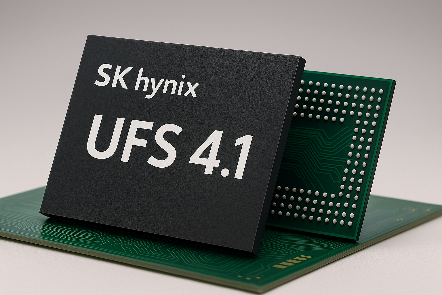
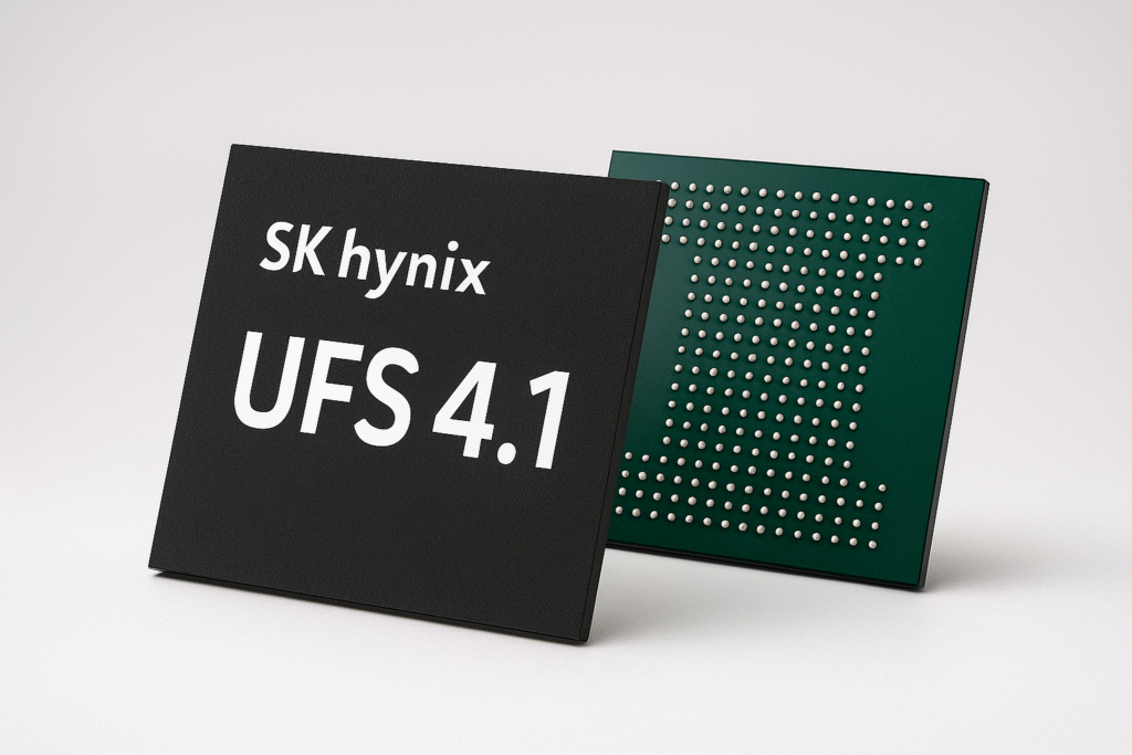
SK Hynix has unveiled the world’s first UFS 4.1 storage solution, built using a groundbreaking 321-layer NAND flash structure. The new SK Hynix UFS 4.1 is designed for premium mobile devices and AI-powered workloads, promising better speed, energy efficiency, and multitasking performance.
Next-Gen Storage Designed for AI
This advanced SK Hynix UFS 4.1 module is optimized for AI-centric devices. Whether it’s live translation, smart photography, or real-time data processing, this chip ensures lightning-fast response directly on-device.
At just 0.85mm thick, it fits ultra-thin phones and foldables while maintaining high performance.
Performance Boost Over UFS 4.0
- 7% higher power efficiency
- 15% faster random read speeds
- 40% faster random write performance
- Sequential read speeds up to 4,300MB/s
These upgrades help improve app loading times, smooth multitasking, and faster AI model execution.
Launch Timeline & Variants
- Capacities: 512GB and 1TB
- Sampling: Ongoing for OEMs
- Mass Production: Early 2026
- Use Cases: Flagship smartphones, AI edge devices, foldables
What This Means for the Industry
With the mobile industry shifting toward smarter, thinner, and more efficient devices, SK Hynix’s UFS 4.1 solution arrives at the perfect time. It supports Snapdragon and Dimensity platforms, making it a strong contender in the flagship storage segment.
Official Statement
“We are on track to expand our position as a full-stack AI memory provider in the NAND space by building a product portfolio with AI technological edge.”
Conclusion
With SK Hynix UFS 4.1, smartphones of 2025 and 2026 can expect faster storage, smoother AI performance, and efficient power usage — all in a compact design. This makes the SK Hynix UFS 4.1 a strong contender for flagship Android devices in 2025.
Stay updated with Mobi4Arena for the latest on chipsets, storage, and smartphone innovations.